


As businesses increasingly integrate artificial intelligence and automation into their operations, the semiconductor industry witnesses significant shifts in design practices, showcasing the importance of emerging technologies and innovative methodologies.
In recent months, businesses across varied sectors have increasingly focused on the integration of artificial intelligence (AI) and automation into their operational frameworks. This trend is reshaping the landscape of business practices, driven by advancements in emerging technologies and industry forecasts suggesting transformative potential.
AI’s influence is particularly pronounced in the semiconductor design and electronic design automation (EDA) fields. Professionals within these industries are witnessing a substantial shift towards new design languages, models, and abstractions. This evolving landscape, often referred to as “Shift Left,” emphasises proactive measures in the design process, enabling engineers to better anticipate challenges rather than responding to them reactively.
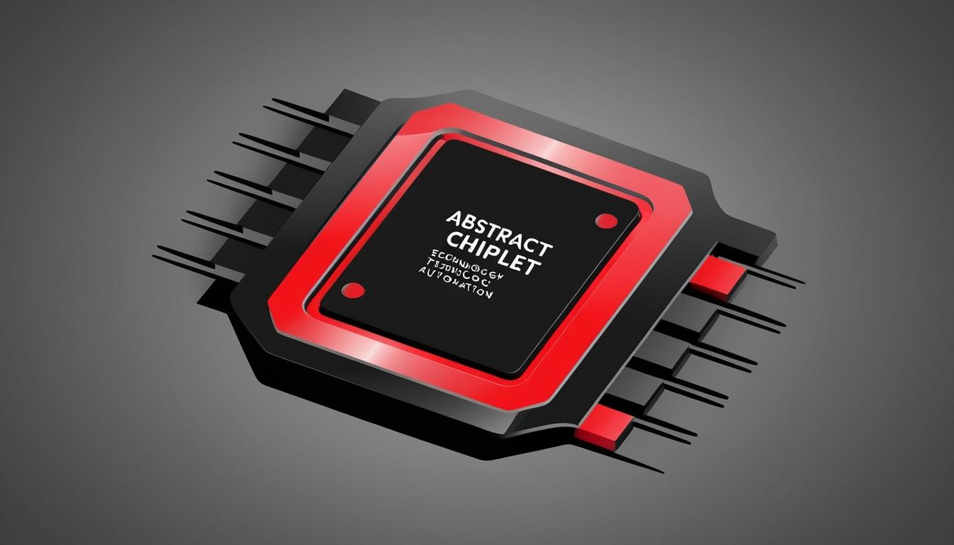
Within this context, the concept of chiplets has emerged as a pivotal development. Chiplet designs allow for the separate production of smaller functional units, offering enhanced performance through tailored assembly for various workloads. Understanding how chiplets interact under diverse conditions is crucial for maintaining signal integrity and optimising performance in heterogeneous designs. The exploration of chiplet architecture not only demonstrates adaptability within technological limits but also introduces a layer of complexity in engineering design.
The ongoing discourse about 3D-integrated circuits (3D-IC) highlights the necessity for balance in modern chip design methodologies. The pros and cons of leveraging a middle-ground assembly method—termed 3.5D—illustrate the trade-offs that engineers consistently navigate between performance and design flexibility.
Moreover, the role of AI in chip design is expanding rapidly, drawing in new startups that aim to streamline processes and reduce the resource burden on engineers. The overarching goal is to free engineers from repetitive tasks, allowing them to focus on more creative and innovative aspects of design.
Forecasts also indicate a future where advancements in extreme ultraviolet lithography (EUV) will play a significant role in optimising chip production. Upcoming technologies, such as high-NA EUV, alongside improved photoresists and etching techniques, are anticipated to enhance performance significantly by refining the intricacies of chip design.
As businesses adapt to these technological advancements, there is a growing need for educational resources tailored to professionals in the field. For instance, materials like “Memory Fundamentals for Engineers” emerge as comprehensive guides, elaborating on memory types, applications, innovations, and their respective limitations. Such resources are pivotal for engineers in cultivating an in-depth understanding necessary for navigating the complexities of modern semiconductor design.
In summary, the landscape of AI automation and semiconductor technology illustrates a dynamic interplay of innovation and adaptation, with industry professionals positioned to harness these emerging trends for enhanced operational efficiency.
Source: Noah Wire Services
- https://calvettiferguson.com/ai-automation-trends-2024/ – This article supports the trend of businesses integrating AI and automation into their operational frameworks, highlighting how AI is transforming business processes and driving efficiency.
- https://mobidev.biz/blog/future-artificial-intelligence-technology-ai-trends – This source discusses the expansion of generative AI and its transformative impact on various industries, aligning with the broader trend of AI adoption in business.
- https://appinventiv.com/blog/ai-trends/ – This article details the rapid advancement of AI technologies, including generative AI, and their impact on business processes and customer interactions, which is relevant to the integration of AI in semiconductor design.
- https://www.charterglobal.com/automation-ai-trends-to-look-out-for-in-2024/ – This source highlights the role of AI in streamlining operations and transforming customer interactions, including the use of generative AI and natural language processing, which can be applied to semiconductor design and automation.
- https://www.pwc.com/us/en/tech-effect/ai-analytics/ai-predictions.html – This article predicts the significant impact of AI, particularly generative AI, on business operations and transformation, which is relevant to the evolving landscape of semiconductor design and automation.
- https://mobidev.biz/blog/future-artificial-intelligence-technology-ai-trends – This source mentions the integration of AI with other technologies like IoT, which can be applied to the design and optimization of semiconductor chips and 3D-integrated circuits.
- https://appinventiv.com/blog/ai-trends/ – This article discusses the use of AI in various industries, including manufacturing and healthcare, which can be extended to the semiconductor industry for optimizing chip design and production.
- https://www.charterglobal.com/automation-ai-trends-to-look-out-for-in-2024/ – This source talks about the role of AI in freeing engineers from repetitive tasks, allowing them to focus on more creative and innovative aspects of design, which is crucial in semiconductor design.
- https://calvettiferguson.com/ai-automation-trends-2024/ – This article emphasizes the importance of educational resources and upskilling for professionals to navigate the complexities of modern technologies, including semiconductor design.
- https://mobidev.biz/blog/future-artificial-intelligence-technology-ai-trends – This source discusses the future of AI technologies, including advancements in software development kits and APIs, which can be applied to the optimization of chip production and design processes.
- https://appinventiv.com/blog/ai-trends/ – This article highlights the integration of AI with IoT and other technologies, which is essential for optimizing chip production and design, including the use of extreme ultraviolet lithography (EUV).


