


The introduction of network-on-chip tiling technology is set to revolutionise semiconductor design, enhancing efficiency and scalability for AI and machine learning systems.
Innovative Network-on-Chip Tiling Transforms Semiconductor Design for AI and Machine Learning
The semiconductor industry is witnessing a significant evolution with the introduction of network-on-chip (NoC) tiling technology, which promises to revolutionise the design and functionality of AI and machine learning-enabled systems. The technique harnesses the capabilities of network-on-chip intellectual property (IP) to effectively manage and scale complex system-on-chip (SoC) designs, enhancing the efficiency and speed of semiconductor development.
The Concept: Modular and Scalable Design
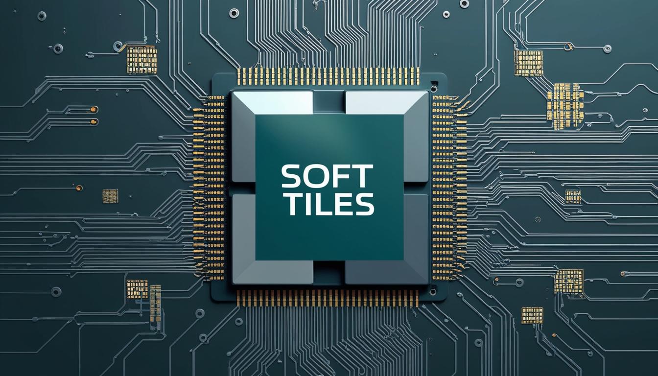
At the heart of this emerging technology is the notion of modularity and scalability. This approach allows SoC architects to construct more efficient and flexible designs through the replication of ‘soft tiles’ across the chip. Each of these soft tiles operates as a self-contained functional unit, making it easier to integrate additional features, verify performance, and optimise components. This modular design approach significantly reduces both design time and associated risks during the semiconductor design process.
Integration with AI and Machine Learning Systems
As the number and complexity of AI-enabled systems grow, so does the demand for efficient processing capabilities. Network-on-chip tiling technology addresses this demand by facilitating the expansion of AI computing power without overhauling existing chip architectures. The addition of soft tiles can be implemented to scale processing capabilities in a systematic and efficient manner, providing a straightforward solution to integrating increasing amounts of AI computational tasks while maintaining system stability and performance.
Mesh Topologies Enhance Design Efficiency
A critical element accompanying the tiling technique is the incorporation of mesh topologies. This combination enhances the ability to manage the connectivity and processing demands of advanced auxiliary processing units (XPUs) within the system. By utilising mesh topologies alongside the modular tiling technique, designers can significantly reduce the time required to design XPU sub-systems and the overall connectivity execution of the SoC.
Implications for the Semiconductor Industry
The implications of NoC tiling for the semiconductor sector are vast. As companies race to integrate AI capabilities more deeply in consumer and industrial products, the ability to quickly scale and develop complex systems becomes invaluable. This innovation not only streamlines the design process but also enhances the performance and capabilities of the end products.
The integration of NoC tiling with mesh topologies is set to reshape semiconductor design landscapes, providing a robust framework for the next generation of AI-enabled devices. As this technology continues to mature, it promises to become a cornerstone in the ongoing evolution of semiconductor development, meeting the growing demands for faster, more efficient, and increasingly complex AI and machine learning applications.
Source: Noah Wire Services


